Enhanced Synaptic Memory Window and Linear Planar In2Se3 Ferroelectric Junctions
The von Neumann computing system has faced a bottleneck between the CPU and memory due to the continuous downscaling of CMOS technology, leading to increased power consumption, and thermal dissipation, and reduced computation speed as data capacity grows. Therefore, an alternative neuromorphic computing system inspired by the biological brain has been proposed.
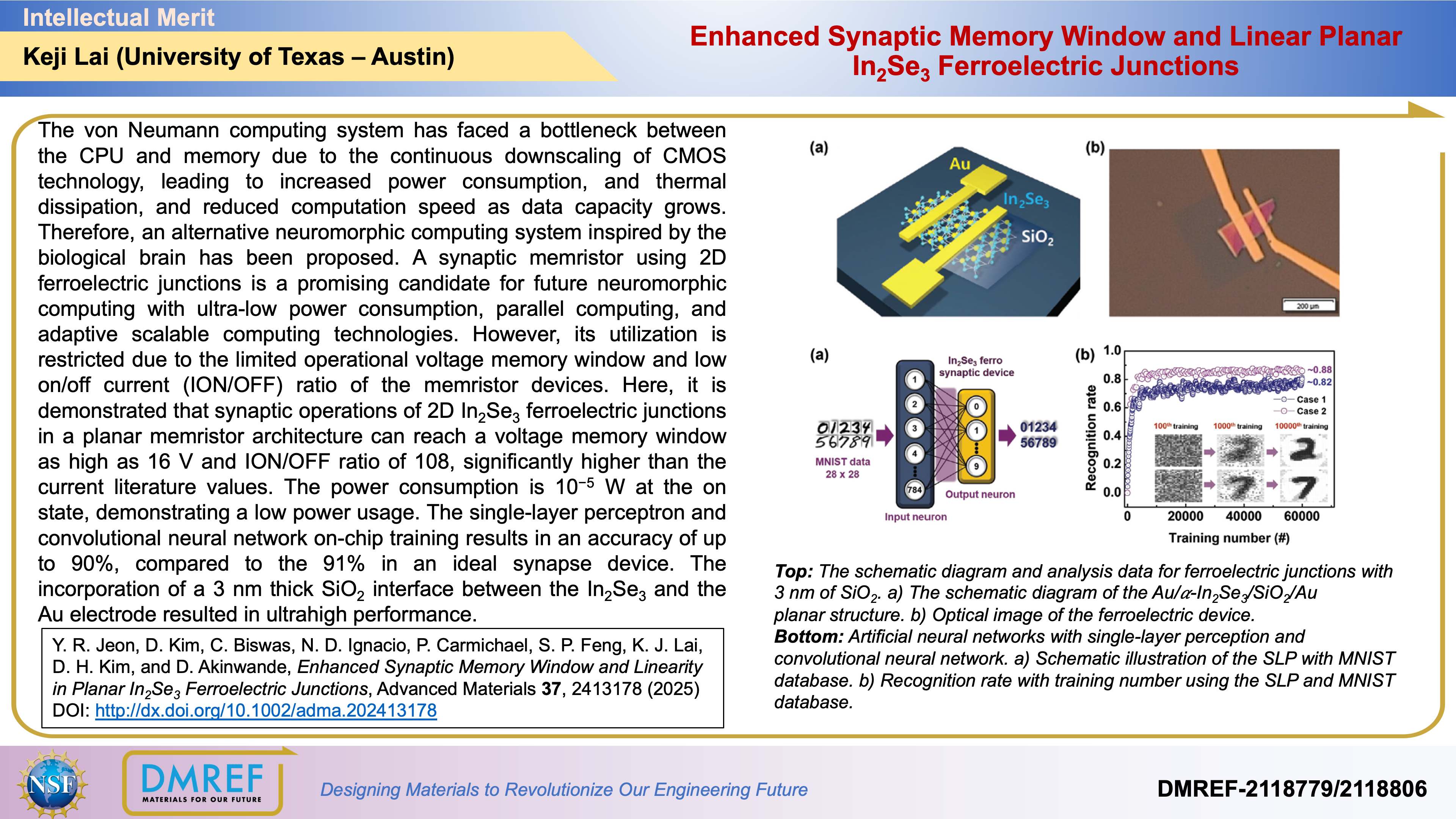
A synaptic memristor using 2D ferroelectric junctions is a promising candidate for future neuromorphic computing with ultra-low power consumption, parallel computing, and adaptive scalable computing technologies. However, its utilization is restricted due to the limited operational voltage memory window and low on/off current (ION/OFF) ratio of the memristor devices.
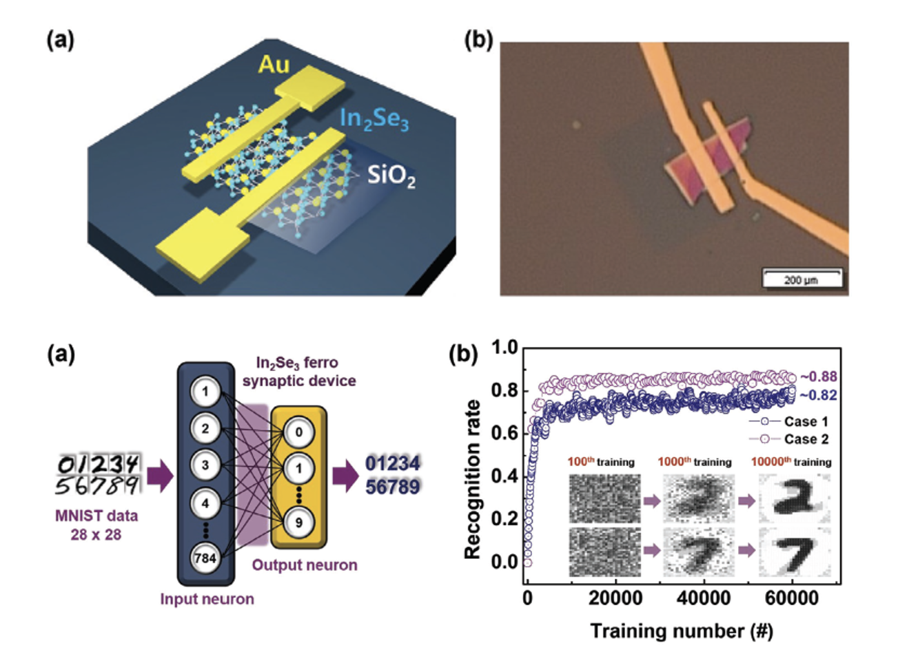
Here, it is demonstrated that synaptic operations of 2D In2Se3 ferroelectric junctions in a planar memristor architecture can reach a voltage memory window as high as 16 V and ION/OFF ratio of 108, significantly higher than the current literature values. The power consumption is 10−5 W at the on state, demonstrating a low power usage. The single-layer perceptron and convolutional neural network on-chip training results in an accuracy of up to 90%, compared to the 91% in an ideal synapse device. The incorporation of a 3 nm thick SiO2interface between the In2Se3 and the Au electrode resulted in ultrahigh performance.