3D Map of Atoms in 2D Materials
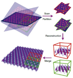
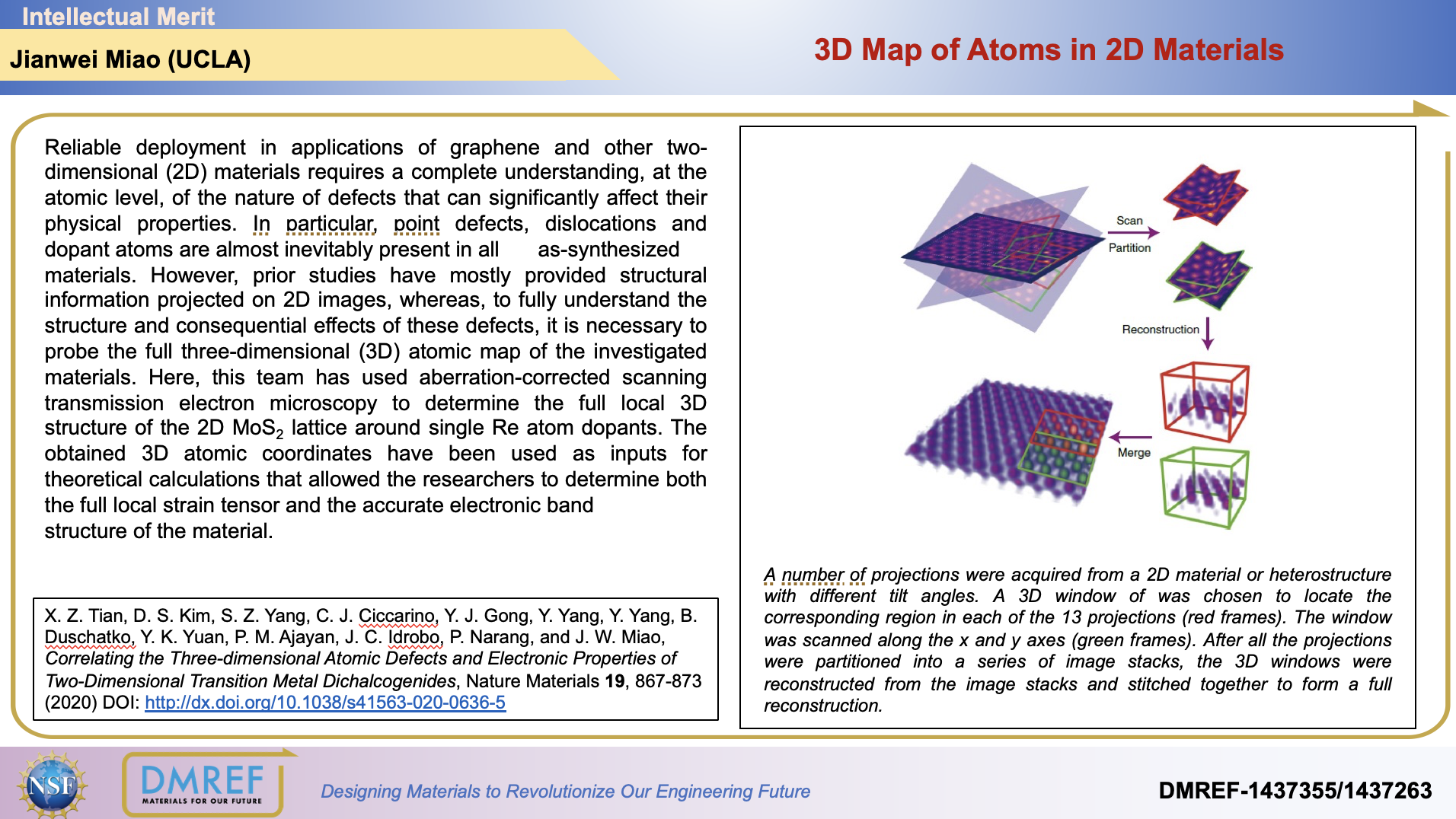
Reliable deployment in applications of graphene and other two-dimensional (2D) materials requires a complete understanding, at the atomic level, of the nature of defects that can significantly affect their physical properties. In particular, point defects, dislocations and dopant atoms are almost inevitably present in all as-synthesized materials. However, prior studies have mostly provided structural information projected on 2D images, whereas, to fully understand the structure and consequential effects of these defects, it is necessary to probe the full three-dimensional (3D) atomic map of the investigated materials. Here, this team has used aberration-corrected scanning transmission electron microscopy to determine the full local 3D structure of the 2D MoS2 lattice around single Re atom dopants. The obtained 3D atomic coordinates have been used as inputs for theoretical calculations that allowed the researchers to determine both the full local strain tensor and the accurate electronic band structure of the material.